
USF Home > College of Arts and Sciences > Physics Department > LAMSAT
LAMSAT Patents
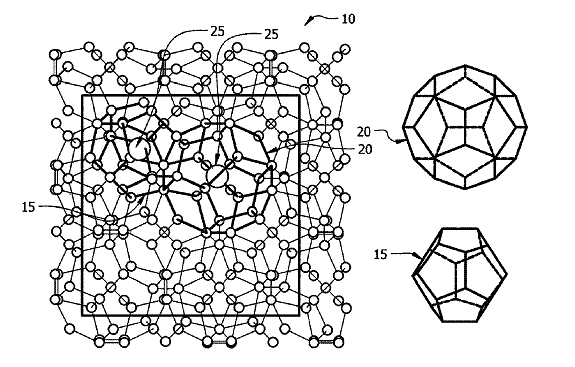
G.S. Nolas, S. Witanachchi and P. Mukherjee, “Clathrate Compounds and Method of Manufacturing”, U.S. Patent No. 7,534,414, May 19, 2009.
The present invention comprises new materials, material structures, and processes of fabrication of such that may be used in technologies involving the conversion of light to electricity and/or heat to electricity, and in optoelectronics technologies. The present invention provide for the fabrication of a clathrate compound comprising a type II clathrate lattice with atoms of silicon and germanium as a main framework forming lattice spacings within the framework, wherein the clathrate lattice follows the general formula Si136-yGey, where y indicates the number of Ge atoms present in the main framework and 136-y indicates the number of Si atoms present in the main framework, and wherein y>0. PDF
P. Mukherjee and S. Witanachchi, “Two-Dimensional Optical Filter and Associated Methods”, U.S. Patent No. 6,697,557 B2, February 24, 2004.
An optical filter includes an input optical fiber bundle and an output fiber bundle. Each of the bundles has one end having the fiber ends substantially two-dimensionally arrayed and another end substantially linearly arrayed. Each input fiber is configured to receive a portion of a two-dimensional input image at the two-dimensional end and transmit the image portion to the one-dimensional end. A spectrally dispersive element receives the image portions from the input fiber bundle and outputs a predetermined spectral component to the output optical fiber bundle at the one-dimensional end, transmitting the image portion to the two-dimensional end. The output fiber bundle two-dimensional ends are arrayed in corresponding fashion to the first ends of the input fibers for spatially reconstructing the input image. PDF

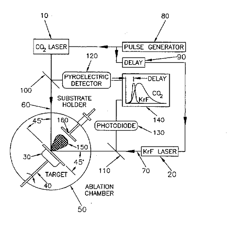
S. Witanachchi and P. Mukherjee, "A Dual-Laser Process for Film Deposition", U.S. Patent No. 5,660,746, August 26, 1997.
The present invention provides a dual-laser deposition process for thin film deposition. Specifically, the present invention provides a method of laser deposition for the growth of in-situ particulate free films. The preferred embodiment includes the spatial overlap on a target of two laser pulses of different wavelengths such that the ejection of the particulates and its subsequent deposition on a substrate during film growth is controlled and essentially eliminated by a suitable temporal delay between the two laser pulses. The present invention enhances the species kinetic energy in the laser-ablated plume via enhanced plume excitation. This allows the reduction of substrate temperature for epitaxial film growth as a result of the increased species mobility on the substrate due to enhanced plume excitation. Also, the ionization in the plume is enhanced. This is important both for enhanced gas phase reactions and for oriented film growth, leading to epitaxy, on the substrate. Moreover, the present invention is designed to enlarge the spatial lateral extent of the plume to enhance the area of uniform thin film deposition on the substrate. PDF
D.T. Shaw, S. Witanachchi, H.S. Kwok, for “Plasma Assisted Laser Deposition of Superconducting Films”, U.S. Patent No. 4,874,741, October 17, 1989
The present invention relates to a method of directly forming a thin, orientated layer, or film, of superconducting materials, suitably mixtures of Pervoskite-type superconducting oxides, on a support base, or substrate, by depositing the layer, or film, in an ionized oxygen atmosphere using a laser beam means. The present process is carried out at temperatures sufficiently high that the film adheres to the substrate, but sufficiently low that a superconducting layer is directly deposited the substrate. Preferably the process is carried out at a temperature less than about 450 degrees C. Temperatures as low as 400 degrees C. have been found useful. PDF